Advanced Interconnect Technology
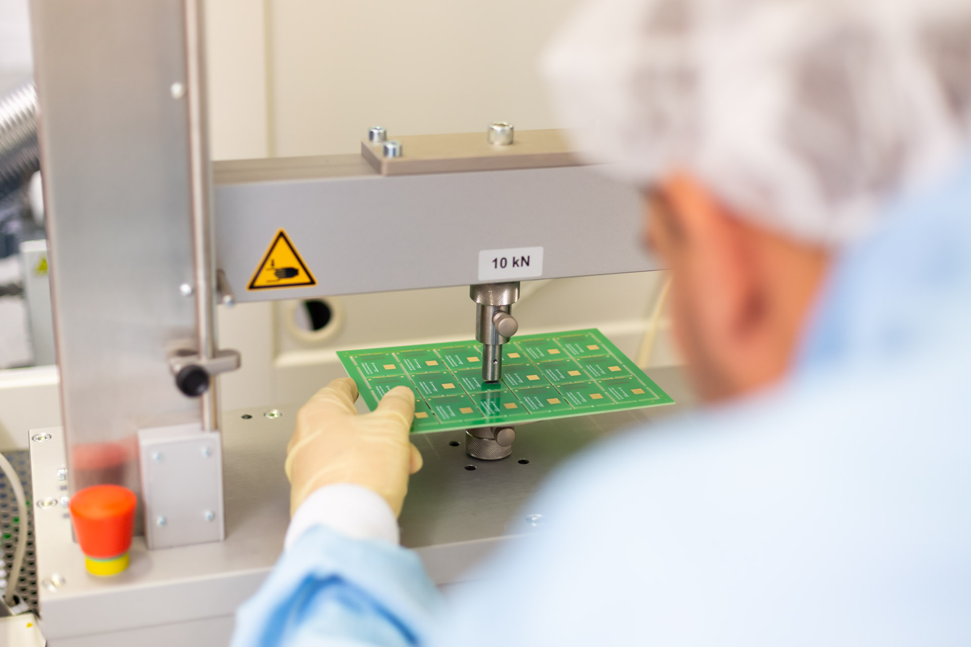
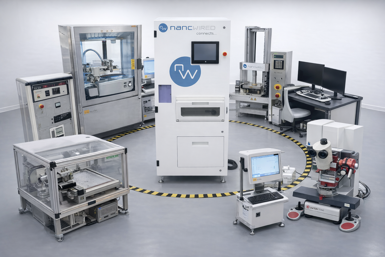
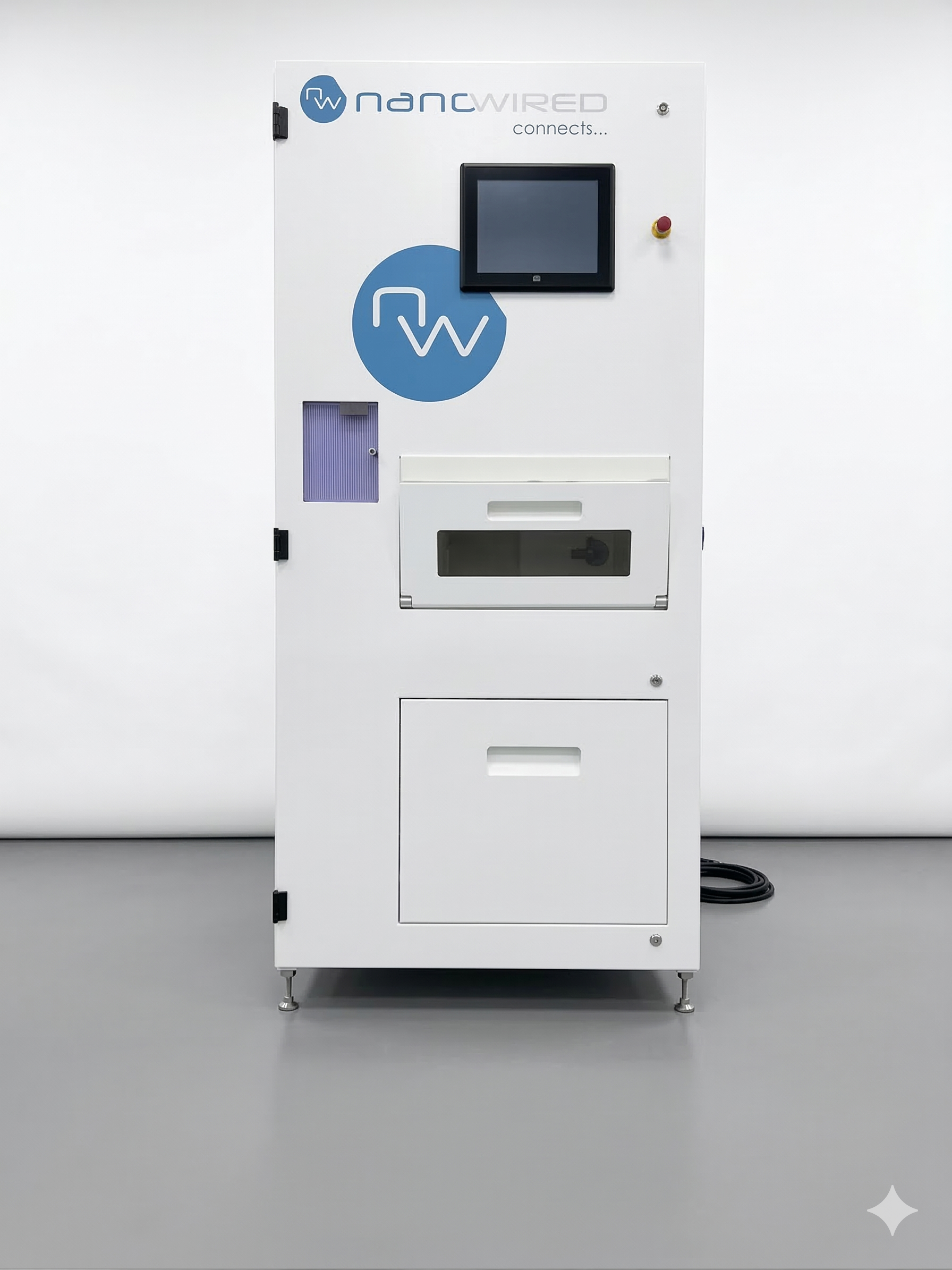
NanoWired GmbH develops nano-scale metallic interconnection systems enabling next-generation semiconductor packaging and room-temperature bonding. Built in Gernsheim, Germany.
Electrochemical growth of metallic nanowires for ultra-high surface bonding density at ambient temperature — no pressure, no heat.
Precision-controlled semiconductor-grade fabrication environment ensuring contamination-free, reproducible nanowire growth at scale.
Advanced materials research and rapid prototyping capabilities for customer-specific interconnect geometry and alloy optimisation.
Low-resistance ohmic contacts enabling higher efficiency switching devices, reduced thermal resistance, and extended lifetime under thermal cycling.
SiC · GaN · Si IGBTRoom-temperature die attachment replacing solder and sintering, with exceptional electrical conductivity and mechanical reliability.
Chiplet · Fan-out · Flip ChipHigh thermal conductivity nanowire pads that conform to microscale surface irregularities — eliminating void formation and delamination.
TIM · Heat Spreader · LidUltra-fine pitch vertical interconnects for stacked die and heterogeneous integration, enabling next-generation 3D-IC architectures.
3D-IC · HBM · CoWoSFounded in Gernsheim, Germany, NanoWired GmbH was established to commercialise breakthrough research in electrochemical nanowire growth. Our technology solves one of the fundamental limits in modern electronics: the need for high-temperature or high-pressure processes to form reliable electrical and thermal bonds.
By growing metallic nanowires directly on substrates, we create millions of micro-contact points that bond at room temperature — enabling assembly of temperature-sensitive devices previously impossible to package reliably.
Work With Us